Is SMIC N+3's Metal Pitch Smaller Than Intel 18A's?
Hacker News•July 24, 2026•10 min read
144 1 12 Share Almost four years ago, we published that SMIC had started shipping 7 nm (N+1) chips . Now, SMIC is shipping its third-generation 7 nm (N+3) process in Huawei’s Kirin 9030, with a minimum metal pitch of 32.5 nm , about 10% tighter than the 36 nm minimum metal pitch shipping in Intel’s latest Panther Lake CPUs on 18A.
The headline is true, but an incomplete cherry picked metric. N+3 reaches the density of TSMC N6 through aggressive DUV multi-patterning and design-technology co-optimization (DTCO), but it pays for that in complexity, efficiency and process control.
We found this and more in our reverse engineering and teardown where we cover SMIC’s N+3 process technology, Huawei’s packaging, memory, architecture, and other exciting features. SemiAnalysis has been building a state-of-the-art teardown lab in Oregon capable of analyzing the world’s most advanced and important chips over the last year and a half. We have already generated revenue on advanced datacenter chip teardowns including our recent reverse engineering of a major TSMC customer’s COUPE CPO optical engine + EIC 3D stack.
This is the first public report from the SemiAnalysis Teardown Engineering & Evaluation Lab, or STEEL for short. The lab is aggressively scaling up and out and we’re excited to announce it publicly. This is a bit of inconvenient timing for TechInsights as they are private equity owned and currently being sold while having enjoyed virtually no credible competition for decades. This has led to TechInsights underinvesting in CAPEX.
SemiAnalysis exceeds TechInsights in revenue despite no venture or private equity ownership and being founded only 6 years ago. Because we have no external investors and are founder-led, we move faster, build faster, and we can release client chip teardowns for free regularly, while focusing on datacenter for our major clients.
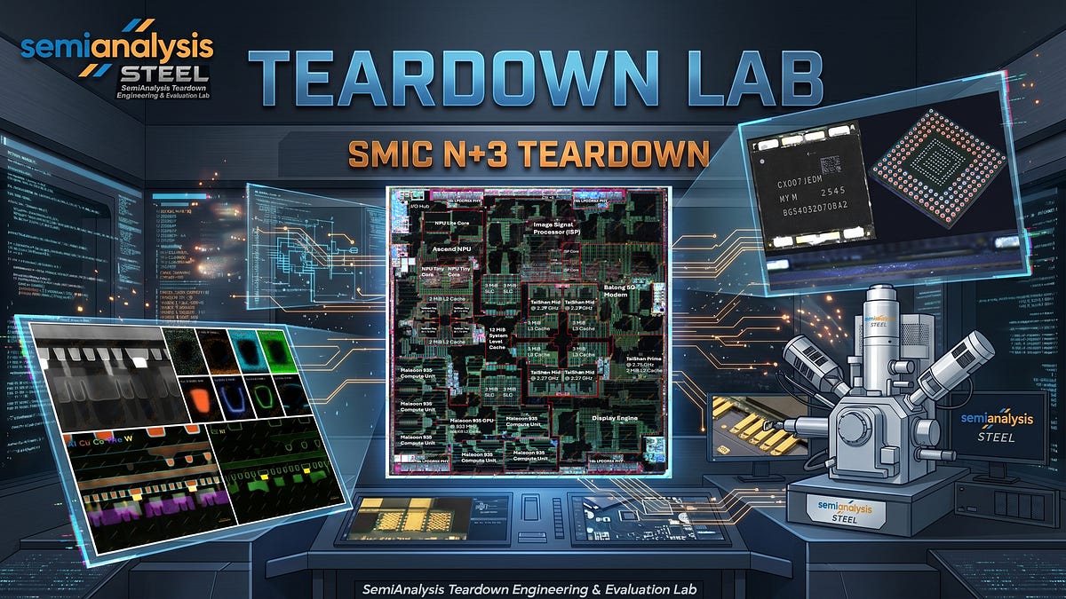
Here’s the first public image from our lab, the HiSilicon Kirin 9030 Pro SoC:
HiSilicon Kirin 9030 die annotation. Source: SemiAnalysis This report will detail our teardown of the Kirin 9030 and our findings on SMIC’s N+3 process, the most advanced in China. For comparison, we’ll show our teardown of the MediaTek Helio G99, made on TSMC N6. Through this comparison, we can look at the effect of export controls – SMIC N+3 and TSMC N6 are comparable nodes, but one is heavily export-controlled, the other free to use the West’s most advanced equipment.
Here we see both China’s progress and constraints. SMIC N+3 reaches TSMC N6-class logic density, but it requires far more aggressive DUV multi-patterning, so it does not match N6 on process maturity or cost. The Kirin 9030 Pro performs similarly to three-year-old Android flagships, and trails far behind the current flagship SoCs from Apple, Qualcomm, MediaTek, and Samsung. The efficiency gap is even wider.
Export controls have not stopped Huawei and SMIC from shipping advanced silicon, but they have forced a different path. Without EUV, SMIC is leaning harder on DUV multi-patterning, DTCO, and increasingly complex integration. The roadmap continues forward through tighter design rules and backside power, but each step adds cost and process risk. Huawei’s τ scaling and LogicFolding show another path: stacking active logic and recovering density through advanced packaging and system-technology co-optimization (STCO).
To understand the Kirin 9030, we must first understand Huawei’s SoC history. HiSilicon is Huawei’s chip design arm, responsible for the Kirin smartphone SoCs, Kunpeng server CPUs, Ascend AI accelerators, and switch/router networking silicon.
Before export controls, Huawei was one of TSMC’s largest customers – the only customer on TSMC’s first EUV node, N7+, and among the first on N5, alongside Apple. That ended in late 2020. Huawei switched to Qualcomm SoCs in its flagship smartphones, though export controls limited them to 4G-only variants.
In late 2023, Huawei returned to in-house silicon with the Kirin 9000s, a successor to the Kirin 9000, fabricated on SMIC N+2 instead of TSMC N5. In the following years, they released the Kirin 9010 and 9020 on the same N+2 process. These chips used Huawei’s in-house TaiShan CPU cores and Maleoon GPU.
We have not torn down a Kirin 9020 ourselves, so the predecessor die shot is from Kurnal. The die shots show how Huawei spent its silicon budget: which functional blocks are where, and how their areas compare to the predecessor.
HiSilicon Kirin 9020 (left) and Kirin 9030 (right) die annotation. Source: Kurnal, SemiAnalysis First, a quick guide to the major blocks on the die.
Kirin 9030 Pro and Kirin 9020 block reference. Source: SemiAnalysis The total die area is nearly identical, but the 9030 uses that area more aggressively. A denser process lets Huawei fit an extra middle CPU core, more GPU and NPU cores, and larger caches into the same footprint.
Kirin 9030 Pro vs Kirin 9020 floorplan analysis. Source: Kurnal, SemiAnalysis In contrast, the Helio G99 is a much smaller, low-cost SoC, built for budget smartphones rather than a flagship device. While the Kirin 9030 is ~140 mm², the G99 is only ~29 mm², roughly one-fifth the area. The underlying TSMC process technology, however, is directly comparable as a baseline for analyzing SMIC’s.
MediaTek Helio G99 die annotation. Source: SemiAnalysis Architecture & PPA The Kirin 9030 is an evolutionary refresh, not a clean-sheet design. Its CPU, GPU and NPU cores carry over the 9020’s families, and the gains come from three levers: the SMIC N+2-to-N+3 process step, DTCO and floorplan work, and incremental microarchitecture. Area is where the first two show up, and the 9030 scales well here. Performance and efficiency are the harder test. Huawei’s design holds up better than its node would suggest, but the chip still trails, both because N+3 sits behind the leading-edge nodes and because its cores, while competent, remain a few generations behind the newest designs.
Kirin 9020 TaiShan V123 (left) and Kirin 9030 TaiShan Prime (right) cores. Source: Kurnal, SemiAnalysis The new prime core is an incremental update. The main changes are a 10% frequency increase from 2.5 GHz to 2.75 GHz and a doubling in the L2 cache from 1 MiB to 2 MiB. Despite the increased cache, the core size decreased by 7.6%. Excluding the private L2 cache, the core size decreased by 21%. This is a large reduction for an incremental node.
Kirin 9020 TaiShan New V120 (left) and Kirin 9030 TaiShan Middle (right) cores. Source: Kurnal, SemiAnalysis Compared with the TaiShan New V120 core in the Kirin 9020, the Kirin 9030’s middle core is almost unchanged architecturally, yet each core shrinks by ~22%. Most of that comes from the move from N+2 to N+3, with layout likely accounting for the rest.
Visually, the most noticeable change is the increase from 3 middle cores to 4. There is also a 20% increase in the shared L3 cache of the big cluster. This helps to improve multi-core performance without sacrificing much in terms of area.
Kirin 9020 (left) and Kirin 9030 (right) Big CPU cluster. Source: Kurnal, SemiAnalysis Even with each core shrinking, the big CPU cluster’s total area is essentially unchanged. The per-core savings went back into an additional middle core and larger caches.
Kirin 9020 (left) and Kirin 9030 (right) TaiShan Tiny cores. Source: Kurnal, SemiAnalysis The tiny cores shrank less than the prime core (excluding its L2 cache) and less than the middle cores. This is likely because fixed overhead is a larger share on a small core. We cannot resolve any architectural changes from the die shot alone, but the per-clock and efficiency gains shown below point to more than pure process and layout scaling. The area reduction was offset by a doubling of the shared L2 cache from 2 MiB to 4 MiB, leaving the total tiny CPU cluster area slightly larger.
Area is the easiest improvement to see from a die shot, but it is only one part of PPA (power, performance, area). For modern logic, power and performance matter just as much, and often more. Since Dennard scaling broke down in the mid-2000s, voltage and frequency have not scaled in step with transistor dimensions, so each node has had to fight harder for gains in performance and efficiency.
Kirin 9030 Pro CPU core performance comparison. Source: Littertree66, SimpleTech, David Huang, SemiAnalysis The starkest comparison is not Kirin 9020 versus Kirin 9030 Pro. Apple’s efficiency cores run circles around Huawei’s prime core. Apple’s low-power core delivers 20% higher integer performance while drawing only 1 W, compared with 4.5 W for Huawei’s prime core. N+3 matches TSMC N6, but N6 is several generations old. Apple and Qualcomm build on N4 and N3P, which are denser and sit on a better voltage-frequency curve, giving them a larger transistor budget and more performance per watt.
The 9030’s own cores did improve. The middle and tiny cores gained 17% and 14% in per-clock integer performance over the 9020, with floating-point flat on the middle core and up 11% on the tiny. The tiny core improves cleanly, with performance rising while power falls and efficiency increases by 45% in integer and 24% in floating point. The middle core is mixed: integer performance rises but power rises faster, cutting integer efficiency by 7%, while lower power lifts floating-point efficiency 16%.
Per-clock gains at the same or lower frequency are microarchitectural, so the cores are tuned, not just shrunk. Both also failed to hold their rated maximum frequencies, pointing to thermal, power, or stability limits. Per clock, the middle core sits around Arm Cortex-A720 and the tiny core near the Cortex-A520; absolute performance trails because Huawei clocks them much lower.
The prime core is roughly Cortex-X2 class per clock, a 2021 design. Apple’s 2020 M1 Firestorm core is still 35% higher per clock and 57% faster in absolute integer performance at a similar 4.5 W. The current leading edge is further ahead again: the Apple M5 P-core is 60% higher per clock and 2.7× faster, the Arm C1 Ultra 45% higher and 2× faster.
Matching older high-end cores per clock is a genuine design achievement. What Huawei cannot match is the voltage-frequency curve and transistor budget of leading-edge nodes, which let Apple, Qualcomm and others spend more transistors in the same area on wider cores, larger caches and deeper buffers while running at lower voltage.
Huawei’s LogicFolding roadmap is one answer, stacking active logic to recover density and shorten signal paths. We return to it later.
Kirin 9020 (left) and Kirin 9030 (right) Maleoon GPU compute units. Source: Kurnal, SemiAnalysis The GPU compute units (CUs) changed more visibly than the CPU cores, moving to a more rectangular layout for both the arithmetic logic unit (ALU) clusters and the CU overall. Even with ray-tracing support added, a CU shrank ~28%.
Kirin 9020 Maleoon 920 (left) and Kirin 9030 Maleoon 935 (right) GPU cluster. Source: Kurnal, SemiAnalysis However, that shrink is offset by the increase from 4 to 6 CUs and the area outside the CUs grew 33%. Overall, the GPU cluster is larger by ~10%.
Kirin 9030 Pro GPU performance comparison. Source: Notebookcheck, SemiAnalysis The GPU is where Huawei makes its biggest gains. The Maleoon 935 is not competitive with current flagships, but it is a large step up from the 920 and reaches older-flagship territory. In 3DMark it is 70% faster in Wild Life Extreme (WLE) and 79% faster in Steel Nomad Light (SNL) than the 920; with 11% higher clocks and 50% more CUs, the ~67% theoretical uplift roughly matches WLE and is beaten by SNL.
It edges ahead of the Snapdragon 8+ Gen 1 in WLE and SNL, and the Dimensity 9200 and Apple A16 in WLE, but stays far behind newer parts: the Snapdragon 8 Elite Gen 5 and Dimensity 9500 are ~2.4–2.6× faster in WLE and ~3.2× faster in SNL.
The Maleoon 935 is Huawei’s first GPU with hardware-accelerated ray tracing; there it lands slightly ahead of the Exynos 2200, and on
 Hacker NewsJuly 24, 202610 min read